Traditional electronic design methods are encountering a new problem when using newer electronic devices that provide a clock based data input or output (for example a MMC or SD memory card via a SPI communication bus). As semiconductor devices have become faster and faster in recent years they have become much more susceptible to issues caused by signal noise. This problem relates to any type of clocked interface where a device you will transfer data to or from automatically moves on to the next data bit, byte or word every time it see’s a new clock edge.
The Problem
For example, a processor or microcontroller is wired to a SD memory card socket to allow it to access an SD memory card via its SPI port. When you try and communicate with the card you know your communicating correctly but the data received is incorrect and the driver doesn’t work correctly, either with the memory card failing to initialise or returning occasional or frequent bad data.
To make matters worse the problem may be sporadic, occurring randomly making tracking down the cause of the problem a nightmare.
Using a logic analyser to monitor the SPI data bus is a good way to try and track down the cause of a problem like this. However when this problem occurs you might find yourself scratching your head looking at the captured data, seeing that the commands sent to the memory card are correct but the data being returned by the card is wrong. Worse still the impedance of your probes may alter the problem causing it to vanish when the probes are connected, or alter its effect.
The Cause
Until relatively recent times digital PCB design (and especially when prototyping) could be viewed as simply a means to electrically interconnect components and unless you designed RF circuits there was little else to worry about. However the PCB itself, or the means of connecting the components used (i.e. prototyping), is now is a very common cause of a loss of signal integrity. The reason is mainly due to the rise and fall times of output signals having decreased as devices are designed to operate faster and faster and to use smaller and smaller silicon manufacturing processes. This problem is not actually due to the operating frequency of a device or the frequency at which a signal is changing, it is due to the speed at which a signal output changes state from high to low and low to high. A signal doesn’t instantaneously change from high to low or low to high, it takes a certain amount of time which will be specified as the rise and fall time in a devices data sheet. Previous signal rise and fall times of many 10’s of nano seconds have now become times measured in just a few nano seconds or for many devices they are measured in pico seconds.
So you may be thinking, this can’t possibly be an issue for me, my board is only operating at a few MHz and I’ve even slowed my data bus down to a few KHz. Well unfortunately that doesn’t matter. If you work with a DC signal the only thing you really care about in a wire or PCB track is its resistance, which for short lengths will be close to zero. However, when using that wire or PCB track with a fast AC signal it starts to behave like a capacitor and inductor. Capacitors and inductors exhibit resistance to alternating current called reactance. The impedance of the wire or track is the vector sum of resistance and reactance, essentially the total resistance seen at a particular frequency. What happens when you send a signal with a fast rising and falling edge down a wire or PCB track, if the impedance of the gate driving the wire or track isn’t exactly the same as the one receiving the it, is it that some of the pulse bounces (literally) back to the driving gate. As there is still an impedance mismatch, the signal continues to bounce between the two until it finally dampens out. This bouncing becomes worse as the speed of signal rise and fall times increases. Basically, the faster rise and fall times of signals from modern semiconductors combined with wire or PCB trace inductance and capacitance causes noise signals of a great magnitude than before. Greater magnitude means the bouncing signals can reach the threshold voltage required for the receiving device to ‘see’ another clock pulse, or an incorrect data level at the moment it is sampling the data line. This captured SPI bus clock transition illustrates the issue:-
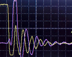
(The timebase is 25nS per square, the voltages are 1V per square and the signals are being sent from a 5V powered microcontroller, to a VHCT125A IC which level converts down to 3.3V for a SD memory card.)
The pink trace is the SPI Data Out (DO) line from a SD memory card and the yellow trace is the SPI Clock (CLK) from a microcontroller. The yellow CLK goes low, the falling edge of which causes the SD memory card to change the state of its pink DO signal to high ready for the next rising clock edge which will clock the data bit into the microcontroller. However, due to CLK falling speed and an impedance mismatch the CLK signal bounces, causing it to rise above the minimum high input level requirement of the VHCT125A. The VHCT125A is a fast device so it faithfully passes the false high signal on to the SD memory card, which is also a fast device and it faithfully responds to the new clock signal, dropping the pink SPI DO signal as the next bit to send is low. End result, as you analyse what the card is returning to you at the microcontroller end it is completely baffling, but if you manage to capture the signals fast enough and at the right time you realise that the card is actually behaving exactly as it should and the problem is being caused by signal noise.
This problem has always occurred with digital signals, but with older semiconductors it could be largely ignored or was not even noticed as the bounce noise was not high enough to be a nuisance, or the recevieing device was not fast enough to detect a brief noise peek. However faster signal rise and fall times have increased the magnitude of this type of noise and devices have generally become faster and faster which now makes it a problem.
Solutions
Design your PCB to use 4 layers or more so you can provide a good ground plane. Using power planes in a PCB design can instantly solve all sorts of signal noise issues. Use impedance calculation tools to work out the correct PCB trace width for a signal in relation to the distance between the signal layer and the power plane layer.
If you can’t use a power plane then at least ensure you provide good ground trace routing. Many PCB designers spend ages optimising the routing of signals on their PCB’s and largely ignore the ground routing, forgetting that the routing of ground signals is 50% of the total path a signal takes.
Add a series resistor between the devices on important signal paths (e.g. 100 ohms – the ideal value is the sum of the resistor and the output impedance of the driver matching the impedance of the PCB trace). This is a popular method that doesn’t drain additional current, but is limited by the problem that the output impedance of a device is often different depending on the output state, and the need to know the PCB trace impedance.
Alternatively add a single terminating resistor to the far end of the PCB trace connected to GND or VCC with a value that matches the characteristic impedance of the trace. All of the energy flowing down the trace is absorbed by the resistor so there is no reflection. Alternatively a pair of resistors, one to GND and the other to VCC can be used. Commonly used values are 220 ohms for the resistor to VCC and 270 ohms for the resistor to ground, causing the trace to ‘see’ a parallel resistance of around 120 ohms. The downside of this is that the pair of resistors draw current so you could instead replace the resistor to GND with a small (couple of hundred pico farad) capacitor.
Once a bit of a black art, designing PCB’s to deal with signal noise issues of this type and many others is now a well understood subject and there are several very good books on the subject. One example is ‘Signal Integrity Issues and Printed Circuit Board Design’ by Douglas Brooks. Although quite mathematical in places if your not mathematically talented it still provides an excellent understanding of these types of issues.
Conclusion
This type of problem crops up all the time and is still often not well understood by both electronic and embedded software designers. Many designers simply give up and never get to the bottom of a problem application. Others find some sort of fix, say by ensuring they use a particular IC or device that seems to work. Often it’s the case its simply an older IC design that has slower signal rise and fall speeds or is slow to detect valid clock edges. Other designers spend ages trying to find the cause, eventually finding it by some clever scoping, or by re-designing their hardware with a ground plane or better routing to provide a more correct trace impedance and the problem disappears. By reading this you are now aware of the problem so the next time you hit a completely unexplainable problem you know what it might be. Hopefully though you’ll make sure you design your hardware better from the outset for pain free development and onward production.